8-Bit CPU – FPGA (Quartus) & PCB Implementation
Overview
Designed and implemented a custom 8-bit CPU to understand processor architecture, instruction execution, and FSM-based control. Extended the design into a PCB-based implementation to explore real-world integration constraints beyond FPGA simulation.
Intel Quartus
FPGA
Custom instruction set
~15 kHz stable clock
PCB bring-up
Phase 1: FPGA Design (Quartus)
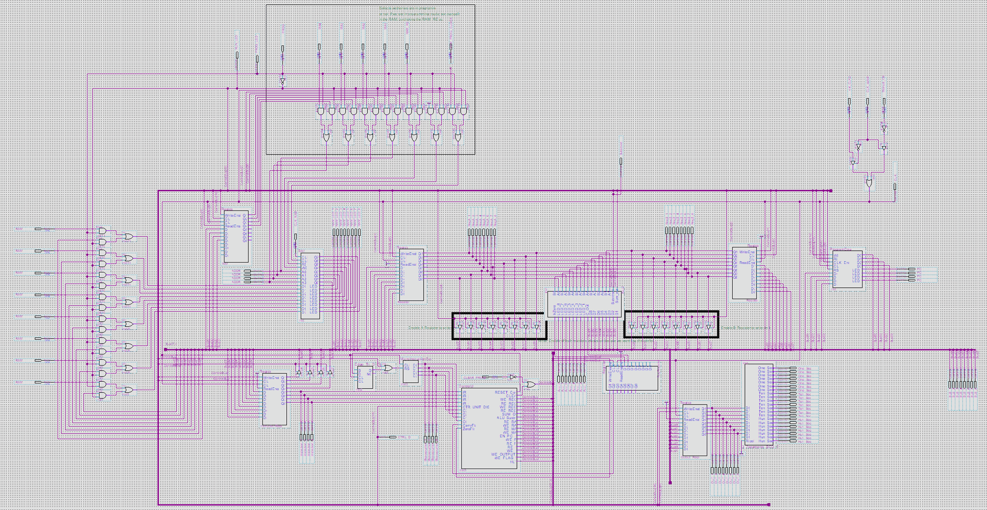
- Designed the datapath and control unit using block-diagram design in Intel Quartus.
- Implemented core components: program counter, registers, RAM, ALU, and control logic.
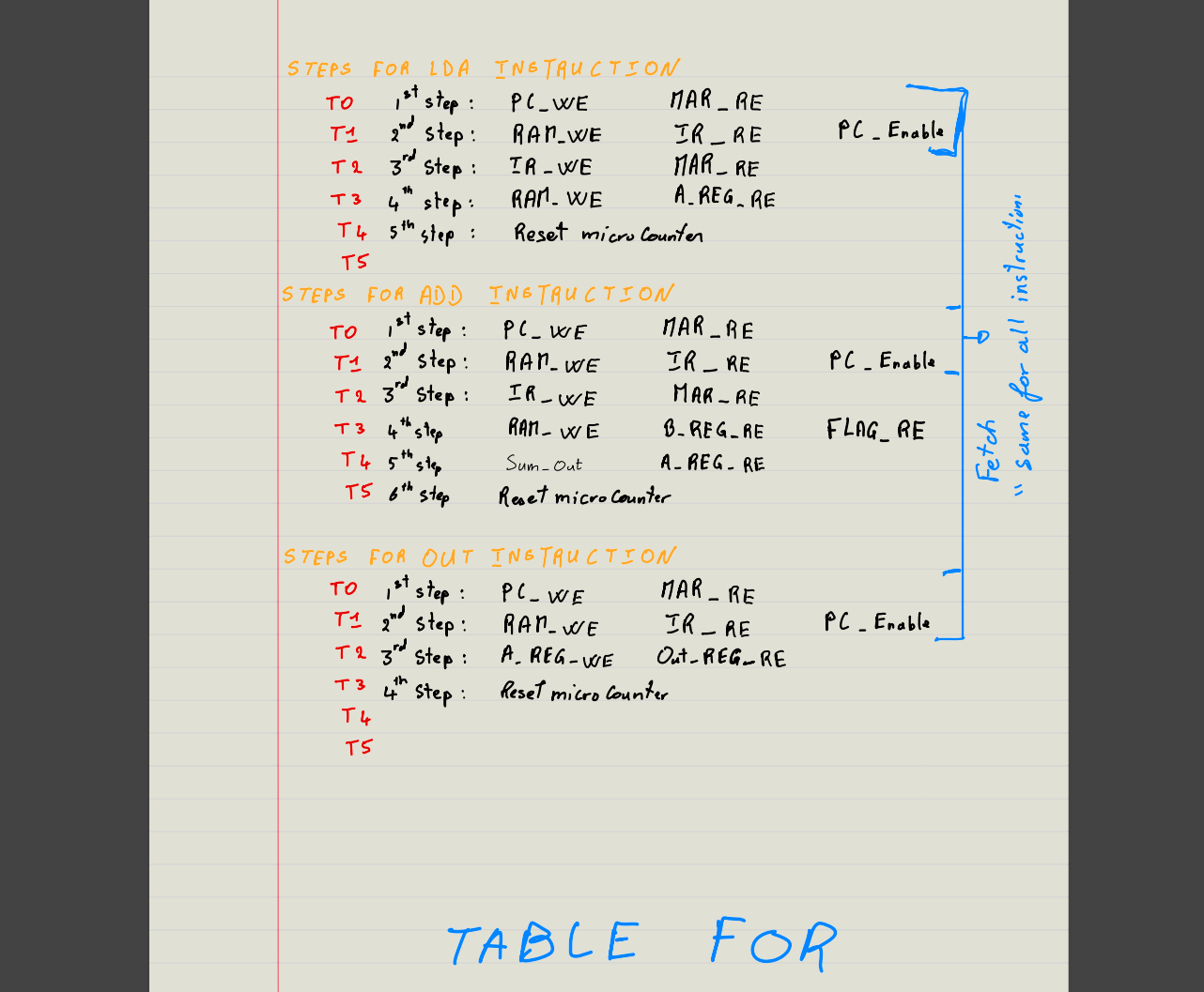
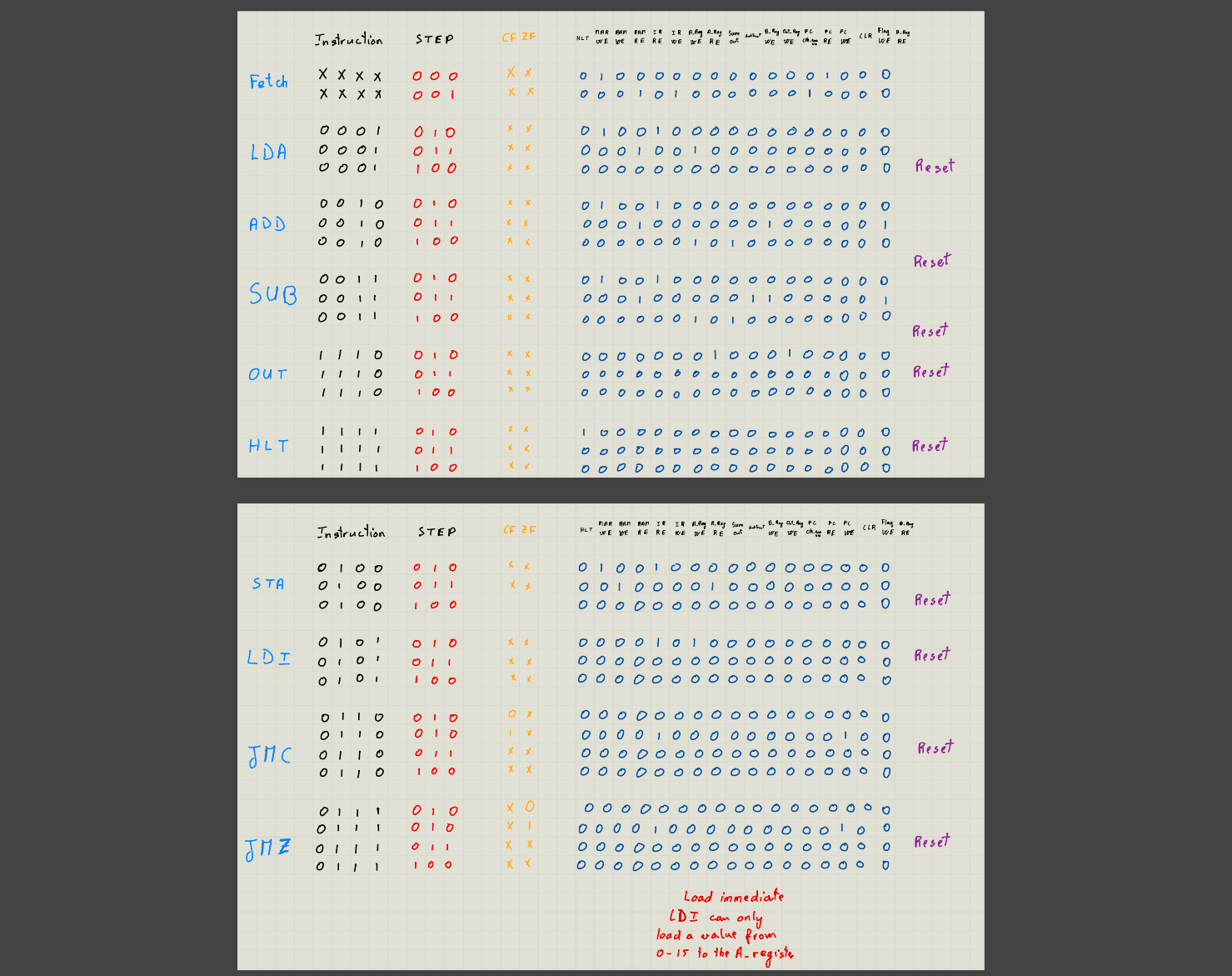
- Defined an instruction set (including addition/subtraction) and validated execution flow.
- Verified functionality using simulation, testbenches, and waveform analysis.
Phase 2: PCB Implementation
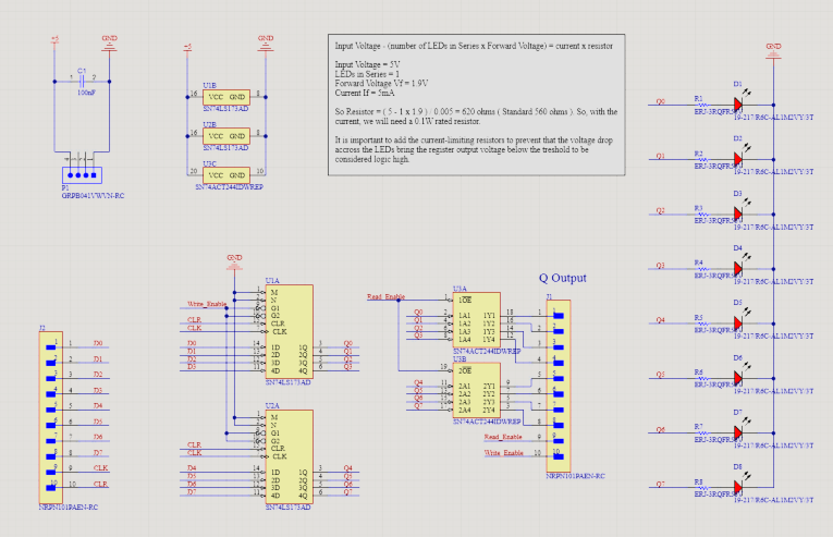
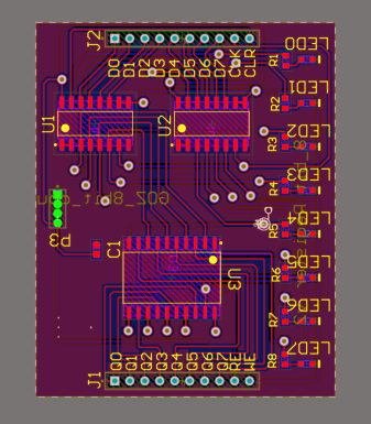
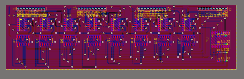
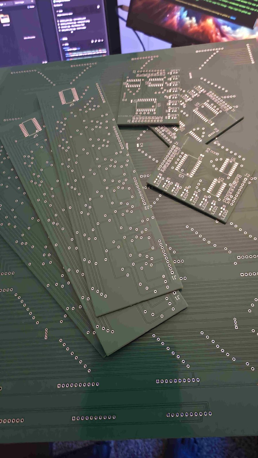
Translated the digital CPU into a PCB-level architecture, working through power and routing considerations that do not appear in FPGA simulation.
Results
- Successfully executed all implemented instructions on FPGA hardware.
- Achieved stable operation at ~15 kHz after resolving timing violations (FPGA).
- Successfully demonstrated CPU operation on a custom PCB.
Waveform + testbench verification of instruction execution
What I Learned
- Hands-on experience with hardware bring-up, debugging, and FPGA vs PCB design tradeoffs.
- Deeper understanding of computer architecture, FSM-based control, and debugging workflow.